The Timing Diagram
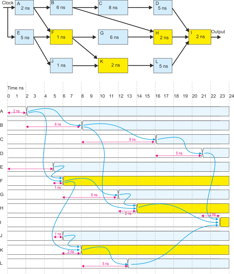
The figure below shows a timing diagram for this system. We have provided traces for the outputs of each of the functional units.
By tradition the two parallel lines indicate that an output can be 0 or 1. It doesn’t
matter. What is of importance in a timing diagram is the point at which signals change
state. This is the cross-
Consider unit A. This has a delay of 2 ns; that is, the output is not valid until at least 2 ns after the input has become valid. The first line in the timing diagram, A, shows that the output of A is valid and remains valid for the remainder of the time. This occurs at 2 ns.
The next trace, B, shows that the output of B becomes valid 6 ns after A is valid or 8 ns after the start of the process.
In order to make the diagram readable, we use cause-
Note that some units have two (or three) inputs. This means that the final output cannot be valid until the latest of the inputs is valid and the additional delay due to the unit has passed. We have used yellow to highlight units with 2 or 3 inputs.
If you look at F, this block has an output from A (valid after 2 ns) and an input form E (valid after 5 ns). Therefore the output from F will not be valid until max(2,5) + 1 = 6 ns. In this timing diagram we have shown all outputs that depend in multiple inputs on yellow.
